- 您现在的位置:买卖IC网 > Sheet目录2008 > MAX1162AEUB+T (Maxim Integrated Products)IC ADC 16BIT 200KSPS 10-MSOP
MAX1162
16-Bit, +5V, 200ksps ADC with 10A
Shutdown
______________________________________________________________________________________
17
Constraints on sequencing the power supplies and
inputs are as follows:
Apply AGND before DGND.
Apply AIN and REF after AVDD and AGND
are present.
DVDD is independent of the supply sequencing.
Ensure that digital return currents do not pass through
the analog ground and that return-current paths are low
impedance. A 5mA current flowing through a PC board
ground trace impedance of only 0.05Ω creates an error
voltage of about 250V, 4LSB error with a +4V full-
scale system.
The board layout should ensure that digital and analog
signal lines are kept separate. Do not run analog and
digital (especially the SCLK and DOUT) lines parallel to
one another. If one must cross another, do so at right
angles.
The ADCs high-speed comparator is sensitive to high-
frequency noise on the AVDD power supply. Bypass an
excessively noisy supply to the analog ground plane
with a 0.1F capacitor in parallel with a 1F to 10F
low-ESR capacitor. Keep capacitor leads short for best
supply-noise rejection.
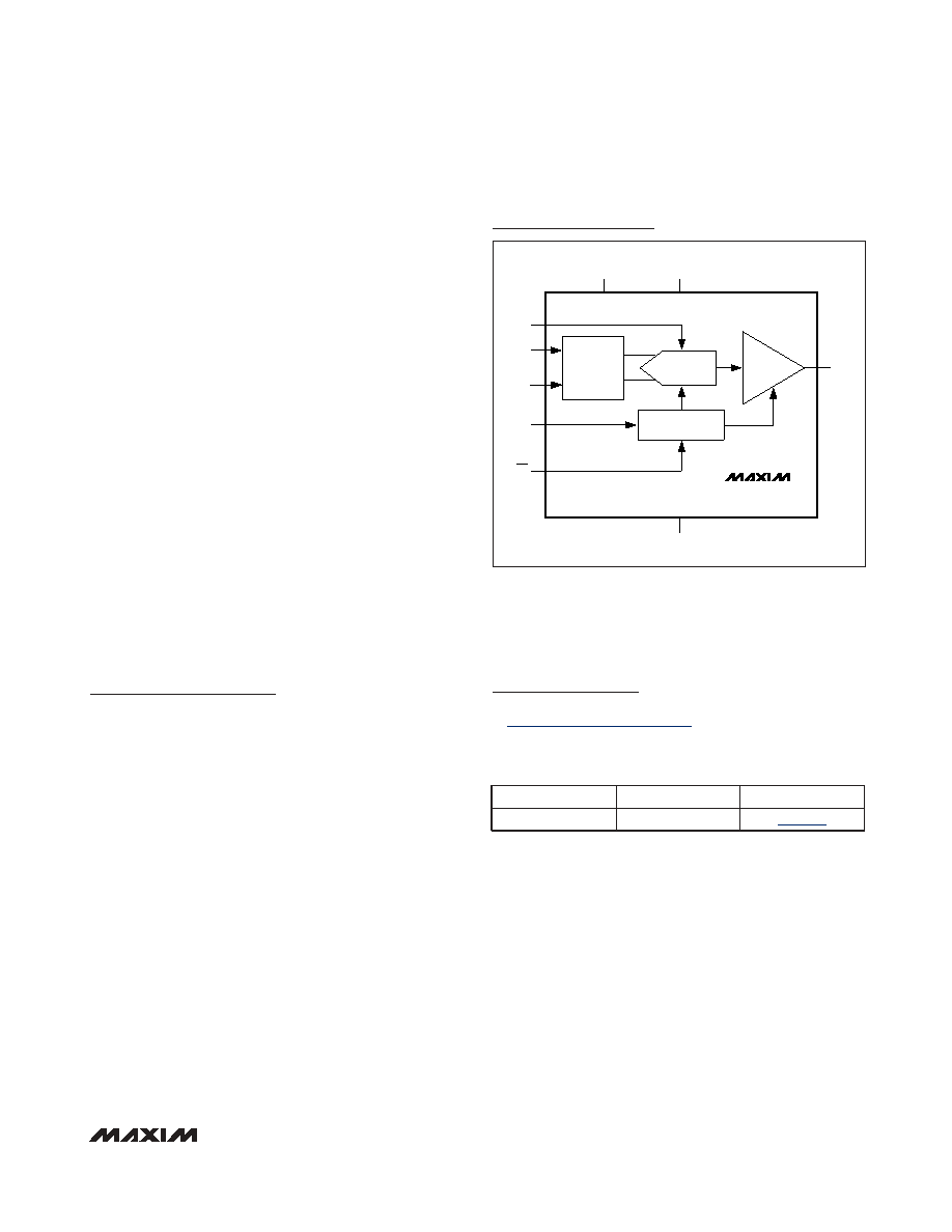
AIN
TRACK AND
HOLD
16-BIT SAR
ADC
CONTROL
DVDD
DGND
CS
AGND
AVDD
REF
DOUT
SCLK
MAX1162
OUTPUT
BUFFER
Functional Diagram
Chip Information
PROCESS: BiCMOS
Package Information
For the latest package outline information and land patterns, go
to www.maxim-ic.com/packages. Note that a “+”, “#”, or “-” in
the package code indicates RoHS status only. Package draw-
ings may show a different suffix character, but the drawing per-
tains to the package regardless of RoHS status.
PACKAGE TYPE
PACKAGE CODE
DOCUMENT NO.
10 MAX
U10-2
发布紧急采购,3分钟左右您将得到回复。
相关PDF资料
MAX11637EEE+T
IC ADC 12BIT 8CH 16QSOP
MAX11643EEG+T
IC ADC 8BIT 8CH 24QSOP
MAX11645EUA+T
IC ADC 12BIT I2C/SRL 1CH 8UMAX
MAX11647EUA+T
IC ADC 10BIT I2C 94.4KSPS 8UMAX
MAX1166BEUP+
IC ADC 16BIT 165KSPS 20-TSSOP
MAX1168BCEG+
IC ADC 16BIT 200KSPS 24-QSOP
MAX1183ECM+TD
IC ADC 10BIT 40MSPS DL 48-TQFP
MAX1184ECM+TD
IC ADC 10BIT 20MSPS DL 48-TQFP
相关代理商/技术参数
MAX1162AEUB-T
功能描述:模数转换器 - ADC RoHS:否 制造商:Texas Instruments 通道数量:2 结构:Sigma-Delta 转换速率:125 SPs to 8 KSPs 分辨率:24 bit 输入类型:Differential 信噪比:107 dB 接口类型:SPI 工作电源电压:1.7 V to 3.6 V, 2.7 V to 5.25 V 最大工作温度:+ 85 C 安装风格:SMD/SMT 封装 / 箱体:VQFN-32
MAX1162BC_B
制造商:MAXIM 制造商全称:Maxim Integrated Products 功能描述:16-Bit, +5V, 200ksps ADC with 10レA Shutdown
MAX1162BCUB
功能描述:模数转换器 - ADC RoHS:否 制造商:Texas Instruments 通道数量:2 结构:Sigma-Delta 转换速率:125 SPs to 8 KSPs 分辨率:24 bit 输入类型:Differential 信噪比:107 dB 接口类型:SPI 工作电源电压:1.7 V to 3.6 V, 2.7 V to 5.25 V 最大工作温度:+ 85 C 安装风格:SMD/SMT 封装 / 箱体:VQFN-32
MAX1162BCUB+
功能描述:模数转换器 - ADC 16-Bit 200ksps 4.096V Precision ADC RoHS:否 制造商:Texas Instruments 通道数量:2 结构:Sigma-Delta 转换速率:125 SPs to 8 KSPs 分辨率:24 bit 输入类型:Differential 信噪比:107 dB 接口类型:SPI 工作电源电压:1.7 V to 3.6 V, 2.7 V to 5.25 V 最大工作温度:+ 85 C 安装风格:SMD/SMT 封装 / 箱体:VQFN-32
MAX1162BCUB+T
功能描述:模数转换器 - ADC 16-Bit 200ksps 4.096V Precision ADC RoHS:否 制造商:Texas Instruments 通道数量:2 结构:Sigma-Delta 转换速率:125 SPs to 8 KSPs 分辨率:24 bit 输入类型:Differential 信噪比:107 dB 接口类型:SPI 工作电源电压:1.7 V to 3.6 V, 2.7 V to 5.25 V 最大工作温度:+ 85 C 安装风格:SMD/SMT 封装 / 箱体:VQFN-32
MAX1162BCUB-T
功能描述:模数转换器 - ADC RoHS:否 制造商:Texas Instruments 通道数量:2 结构:Sigma-Delta 转换速率:125 SPs to 8 KSPs 分辨率:24 bit 输入类型:Differential 信噪比:107 dB 接口类型:SPI 工作电源电压:1.7 V to 3.6 V, 2.7 V to 5.25 V 最大工作温度:+ 85 C 安装风格:SMD/SMT 封装 / 箱体:VQFN-32
MAX1162BE_B
制造商:MAXIM 制造商全称:Maxim Integrated Products 功能描述:16-Bit, +5V, 200ksps ADC with 10レA Shutdown
MAX1162BEUB
功能描述:模数转换器 - ADC RoHS:否 制造商:Texas Instruments 通道数量:2 结构:Sigma-Delta 转换速率:125 SPs to 8 KSPs 分辨率:24 bit 输入类型:Differential 信噪比:107 dB 接口类型:SPI 工作电源电压:1.7 V to 3.6 V, 2.7 V to 5.25 V 最大工作温度:+ 85 C 安装风格:SMD/SMT 封装 / 箱体:VQFN-32